- 您现在的位置:买卖IC网 > Sheet目录337 > LH28F320S3HNS-ZM (Sharp Microelectronics)IC FLASH 32MBIT 110NS 56SSOP
�� �
�
�LHF32KZM�
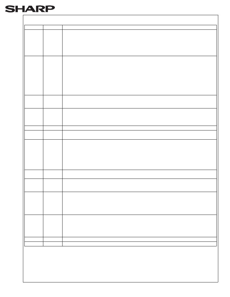
�Table� 2.� Pin� Descriptions�
�5�
�Symbol�
�A� 0� -A� 21�
�DQ� 0� -DQ� 15�
�CE� 0� #,�
�CE� 1� #�
�RP#�
�OE#�
�WE#�
�STS�
�WP#�
�BYTE#�
�V� PP�
�V� CC�
�GND�
�NC�
�Type�
�INPUT�
�INPUT/�
�OUTPUT�
�INPUT�
�INPUT�
�INPUT�
�INPUT�
�OPEN�
�DRAIN�
�OUTPUT�
�INPUT�
�INPUT�
�SUPPLY�
�SUPPLY�
�SUPPLY�
�Name� and� Function�
�ADDRESS� INPUTS:� Inputs� for� addresses� during� read� and� write� operations.� Addresses� are�
�internally� latched� during� a� write� cycle.�
�A� 0� :� Byte� Select� Address.� Not� used� in� x16� mode(can� be� floated).�
�A� 1� -A� 4� :� Column� Address.� Selects� 1� of� 16� bit� lines.�
�A� 5� -A� 15� :� Row� Address.� Selects� 1� of� 2048� word� lines.�
�A� 16� -A� 21� :� Block� Address.�
�DATA� INPUT/OUTPUTS:�
�DQ� 0� -DQ� 7� :Inputs� data� and� commands� during� CUI� write� cycles;� outputs� data� during� memory�
�array,� status� register,� query,� and� identifier� code� read� cycles.� Data� pins� float� to� high-�
�impedance� when� the� chip� is� deselected� or� outputs� are� disabled.� Data� is� internally� latched�
�during� a� write� cycle.�
�DQ� 8� -DQ� 15� :Inputs� data� during� CUI� write� cycles� in� x16� mode;� outputs� data� during� memory�
�array� read� cycles� in� x16� mode;� not� used� for� status� register,� query� and� identifier� code� read�
�mode.� Data� pins� float� to� high-impedance� when� the� chip� is� deselected,� outputs� are�
�disabled,� or� in� x8� mode(Byte#=V� IL� ).� Data� is� internally� latched� during� a� write� cycle.�
�CHIP� ENABLE:� Activates� the� device’s� control� logic,� input� buffers� decoders,� and� sense�
�amplifiers.� Either� CE� 0� #� or� CE� 1� #� V� IH� deselects� the� device� and� reduces� power� consumption�
�to� standby� levels.� Both� CE� 0� #� and� CE� 1� #� must� be� V� IL� to� select� the� devices.�
�RESET/DEEP� POWER-DOWN:� Puts� the� device� in� deep� power-down� mode� and� resets�
�internal� automation.� RP#� V� IH� enables� normal� operation.� When� driven� V� IL� ,� RP#� inhibits�
�write� operations� which� provides� data� protection� during� power� transitions.� Exit� from� deep�
�power-down� sets� the� device� to� read� array� mode.�
�OUTPUT� ENABLE:� Gates� the� device’s� outputs� during� a� read� cycle.�
�WRITE� ENABLE:� Controls� writes� to� the� CUI� and� array� blocks.� Addresses� and� data� are�
�latched� on� the� rising� edge� of� the� WE#� pulse.�
�STS� (RY/BY#):� Indicates� the� status� of� the� internal� WSM.� When� configured� in� level� mode�
�(default� mode),� it� acts� as� a� RY/BY#� pin.� When� low,� the� WSM� is� performing� an� internal�
�operation� (block� erase,� full� chip� erase,� (multi)� word/byte� write� or� block� lock-bit�
�configuration).� STS� High� Z� indicates� that� the� WSM� is� ready� for� new� commands,� block�
�erase� is� suspended,� and� (multi)� word/byte� write� is� inactive,� (multi)� word/byte� write� is�
�suspended� or� the� device� is� in� deep� power-down� mode.� For� alternate� configurations� of� the�
�STATUS� pin,� see� the� Configuration� command.�
�WRITE� PROTECT:� Master� control� for� block� locking.� When� V� IL,� Locked� blocks� can� not� be�
�erased� and� programmed,� and� block� lock-bits� can� not� be� set� and� reset.�
�BYTE� ENABLE:� BYTE#� V� IL� places� device� in� x8� mode.� All� data� is� then� input� or� output� on�
�DQ� 0-7� ,� and� DQ� 8-15� float.� BYTE#� V� IH� places� the� device� in� x16� mode� ,� and� turns� off� the� A� 0�
�input� buffer.�
�BLOCK� ERASE,� FULL� CHIP� ERASE,� (MULTI)� WORD/BYTE� WRITE,� BLOCK� LOCK-�
�BIT� CONFIGURATION� POWER� SUPPLY:� For� erasing� array� blocks,� writing� bytes� or�
�configuring� block� lock-bits.� With� V� PP� ≤� V� PPLK� ,� memory� contents� cannot� be� altered.� Block�
�erase,� full� chip� erase,� (multi)� word/byte� write� and� block� lock-bit� configuration� with� an� invalid�
�V� PP� (see� DC� Characteristics)� produce� spurious� results� and� should� not� be� attempted.�
�DEVICE� POWER� SUPPLY:� Internal� detection� configures� the� device� for� 2.7V� or� 3.3V�
�operation.� To� switch� from� one� voltage� to� another,� ramp� V� CC� down� to� GND� and� then� ramp�
�V� CC� to� the� new� voltage.� Do� not� float� any� power� pins.� With� V� CC� ≤� V� LKO� ,� all� write� attempts� to�
�the� flash� memory� are� inhibited.� Device� operations� at� invalid� V� CC� voltage� (see� DC�
�Characteristics)� produce� spurious� results� and� should� not� be� attempted.�
�GROUND:� Do� not� float� any� ground� pins.�
�NO� CONNECT:� Lead� is� not� internal� connected;� it� may� be� driven� or� floated.�
�Rev.� 1.6�
�发布紧急采购,3分钟左右您将得到回复。
相关PDF资料
LH28F320SKTD-ZR
IC FLASH 32MBIT 70NS 48TSOP
LHF00L28
IC FLASH 16MBIT 70NS 48TSOP
LPM409 CHASSIS
STNRD 4SLOT CHASSIS W/INPUT LEAD
LS15RB1201J04
POE SPLITTER 10.8W 12V @0.9A
LT1932ES6#TRMPBF
IC LED DRIVR WHITE BCKLGT TSOT-6
LT1937ES5#TRMPBF
IC LED DRIVR WHITE BCKLGT TSOT-5
LT3003EMSE#TRPBF
IC LED DRIVER BALLASTER 10-MSOP
LT3465AES6#TRMPBF
IC LED DRIVR WHITE BCKLGT TSOT-6
相关代理商/技术参数
LH28F320S3-L11
制造商:SHARP 制造商全称:Sharp Electrionic Components 功能描述:32-MBIT(4MBx8/2MBx16)Smart 3 Flash MEMORY
LH28F320S3-L110
制造商:SHARP 制造商全称:Sharp Electrionic Components 功能描述:32-MBIT(4MBx8/2MBx16)Smart 3 Flash MEMORY
LH28F320S3-L130
制造商:SHARP 制造商全称:Sharp Electrionic Components 功能描述:32-MBIT(4MBx8/2MBx16)Smart 3 Flash MEMORY
LH28F320S3-L14
制造商:SHARP 制造商全称:Sharp Electrionic Components 功能描述:32-MBIT(4MBx8/2MBx16)Smart 3 Flash MEMORY
LH28F320S3-L140
制造商:SHARP 制造商全称:Sharp Electrionic Components 功能描述:32-MBIT(4MBx8/2MBx16)Smart 3 Flash MEMORY
LH28F320S3-L160
制造商:SHARP 制造商全称:Sharp Electrionic Components 功能描述:32-MBIT(4MBx8/2MBx16)Smart 3 Flash MEMORY
LH28F320S3NS
制造商:SHARP 制造商全称:Sharp Electrionic Components 功能描述:Smart voltage 32Mbit Flash Memory
LH28F320S3NS-L11
功能描述:IC FLASH 32MBIT 110NS 56SSOP RoHS:否 类别:集成电路 (IC) >> 存储器 系列:- 标准包装:60 系列:- 格式 - 存储器:EEPROMs - 串行 存储器类型:EEPROM 存储容量:16K (2K x 8) 速度:2MHz 接口:SPI 3 线串行 电源电压:2.5 V ~ 5.5 V 工作温度:-40°C ~ 85°C 封装/外壳:8-DIP(0.300",7.62mm) 供应商设备封装:8-PDIP 包装:管件 产品目录页面:1449 (CN2011-ZH PDF)